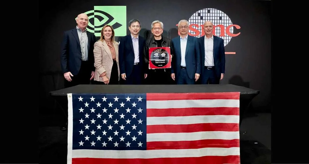
On October 17, 2025, the first NVIDIA Blackwell wafer was officially produced at TSMC's Arizona factory in Phoenix. NVIDIA founder and CEO Jensen Huang visited in person and, signing the first Blackwell wafer alongside TSMC VP Y.L. Wang, declared it "Act 2 of the industrial revolution of the AI era."
"This isn't just a chip. This is the moment when the most important technology industry in American history returns as the most important manufacturing industry." — Jensen Huang
The event is not just a semiconductor manufacturing milestone. Behind it lies America's AI/semiconductor supply chain restructuring strategy. Over the past decade, NVIDIA designs chips in the US while actual production occurs mostly at TSMC (Taiwan) or Samsung (Korea). The US-China technology hegemony competition escalating prompted a shift to "reshoring" AI chip production domestically. TSMC Arizona — over $40 billion invested under the CHIPS and Science Act — symbolizes America's return as an "AI semiconductor manufacturing powerhouse."
NVIDIA's Blackwell architecture covers AI training, inference, robotics, and digital twins as a next-generation AI computing engine. This chip delivers 2.5x the performance of the previous Hopper, 30% power efficiency improvement, and 4x LLM inference speed. TSMC Arizona will produce 2nm-4nm processes and next-generation A16 chips — serving as the core Physical Layer of global AI infrastructure.
This development simultaneously achieves three effects: physically relocating AI industry supply chains to the US, returning high-end manufacturing jobs, and securing data sovereignty and tech security. TSMC Arizona is also the core puzzle of America's longstanding pursuit of "distributing Taiwan dependency + rebuilding technology alliances." Jensen Huang captured the moment: "AI is a new manufacturing industry. It's the industrial revolution that converts data into intelligence."